基于ADI ADP230x 的1.2A超小型電流模式DC電源

ADI 公司的ADP2300/ADP2301是集成了功率MOSFET的小型緊湊固定頻率電流模式降壓DC/DC電源穩壓器, 輸入電壓VIN從3V到20V,輸出電壓從0.8V到0.85xVIN,效率高達91%,可選擇開關頻率700 kHz (ADP2300) 或1.4 MHz (ADP2301) ,超小型6引腳TSOT封裝,主要用在系統內部電源轉換,通信和網絡設備,工業和儀表,保健和醫療設備以及消費類電子產品.本文介紹ADP2300/ADP2301主要特性,方框圖,以及多種應用電路.
The ADP2300/ADP2301 are compact, constant-frequency, current-mode, step-down dc-to-dc regulators with integrated power MOSFET. The ADP2300/ADP2301 devices run from input voltages of 3.0 V to 20 V, making them suitable for a wide range of applications. A precise, low voltage internal reference makes these devices ideal for generating a regulated output voltage as low as 0.8 V, with ±2% accuracy, for up to 1.2 A load current.
There are two frequency options: the ADP2300 runs at 700 kHz, and the ADP2301 runs at 1.4 MHz. These options allow users to make decisions based on the trade-off between efficiency and total solution size. Current-mode control provides fast and stable line and load transient performance. The ADP2300/ADP2301 devices include internal soft start to prevent inrush current at power-up. Other key safety features include short-circuit protec-tion, thermal shutdown (TSD), and input undervoltage lockout (UVLO). The precision enable pin threshold voltage allows the ADP2300/ADP2301 to be easily sequenced from other input/ output supplies. It can also be used as a programmable UVLO input by using a resistive divider.
The ADP2300/ADP2301 are available in a 6-lead TSOT package and are rated for the ?40℃ to +125℃ junction temperature range.
ADP2300/ADP2301主要特性:
1.2 A maximum load current
±2% output accuracy over temperature range
Wide input voltage range: 3.0 V to 20 V
700 kHz (ADP2300) or 1.4 MHz (ADP2301) switching frequency options
High efficiency up to 91%
Current-mode control architecture
Output voltage from 0.8 V to 0.85 × VIN
Automatic PFM/PWM mode switching
Precision enable pin with hysteresis
Integrated high-side MOSFET
Integrated bootstrap diode
Internal compensation and soft start
Minimum external components
Undervoltage lockout (UVLO)
Overcurrent protection (OCP) and thermal shutdown (TSD)
ADIsimPower? online design tool
Available in ultrasmall, 6-lead TSOT package
ADP2300/ADP2301應用:
LDO replacement for digital load applications
Intermediate power rail conversion
Communications and networking
Industrial and instrumentation
Healthcare and medical
Consumer
圖1。ADP2300/ADP2301功能方框圖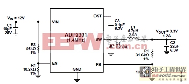
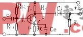
圖2。ADP2300/ADP2301設計案例電路圖
推薦的輸出電流1.2A外接元件表:

圖3.推薦的ADP2300/ADP2301PCB布局圖
典型應用電路圖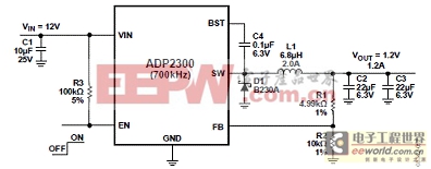
圖4.ADP2300—700 kHz 典型應用(帶外接使能): VIN = 12 V, VOUT = 1.2 V/1.2 A 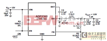
圖5.ADP2300—700 kHz 典型應用(帶外接使能): VIN = 12 V, VOUT = 1.8 V/1.2 A 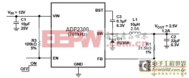
圖6.ADP2300—700 kHz 典型應用(帶外接使能): VIN = 12 V, VOUT = 2.5V/1.2 A 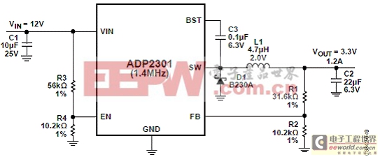
圖7.ADP2301—1.4MHz 典型應用(帶可編7.8V起動輸入電壓): VIN = 12 V, VOUT = 3.3 V/1.2 A 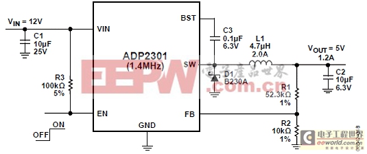
圖8.ADP2301—1.4Hz 典型應用(帶外接使能): VIN = 12 V, VOUT = 5.0 V/1.2 A 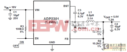
圖9.ADP2301—1.4Hz 典型應用(帶外接使能): VIN = 18 V, VOUT = 5.0 V/1.2 A 
圖10.ADP2301—1.4Hz 典型應用(帶外接使能): VIN = 9 V, VOUT = 3.3 V/1.2 A 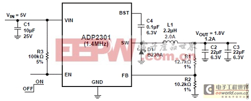
圖11.ADP2301—1.4Hz 典型應用(帶外接使能): VIN = 5 V, VOUT = 1.8 V/1.2 A


評論